Marvell · 2026
3nm
Next-gen hyperscaler switch ASIC. I built the product engineering plan that maps its path to mass production.
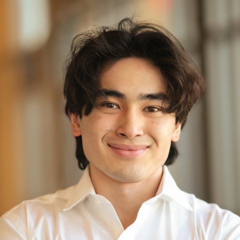
Electrical Engineering at UC San Diego
From atoms to ASICs.
I've fabricated photonic and semiconductor devices at Harvard and Stanford, grown and characterized doped epitaxial films at Applied Materials, and planned a 3nm ASIC’s path to mass production at Marvell.
300 mm wafer, rendered in code.
Marvell · 2026
3nm
Next-gen hyperscaler switch ASIC. I built the product engineering plan that maps its path to mass production.
Published.
Co-author in Optica, 2026. Dynamic control of intrinsic optical chirality via MEMS-integrated photonic crystals, from my summer in Harvard's Mazur Group.
Read the paperSi · SiGe · Ge · SiGeBC
Epitaxial films I ran baseline recipes for on Centura RPCVD tools at Applied Materials.
6
Internships across research labs and industry since 2022.
3
Cleanrooms. Stanford, Harvard, and UC San Diego.
Overview
Chips pass through many hands before they ship. I've worked at five of those stages, from simulation to production test.
Harvard · Capasso Group
FDTD · MATLAB
Stanford SNF · Harvard Mazur Group
E-beam · RIE · DRIE
Applied Materials
RPCVD epitaxy
Qualcomm Institute · Applied Materials
SEM · XRD · JMP
Marvell
WS · SLT · ATE · MPR
Industry
One in equipment R&D, growing and measuring epitaxial films. One in product engineering, getting a 3nm ASIC ready for volume.
Marvell Technology · Summer 2026
Product Engineering Intern, Hyperscaler ASIC & Custom Compute.
Try it · Plan a path to mass production
Critical path: WS → SLT → HVM
Drag a bar to delay it, or drag its right edge to change its length. Illustrative schedule, not Marvell data.
Applied Materials · Summer 2025
Process Engineering Intern, Silicon Epitaxy R&D.
Try it · Grow a SiGe film on silicon
Research
Four labs on two coasts, from Stanford's shared cleanroom to Harvard's photonics groups.
Harvard SEAS · Mazur Group · 2024
Stanford Nanofabrication Facility · 2022–24
Harvard SEAS · Capasso Group · 2023
UC San Diego · Qualcomm Institute · 2024–25
Try it
In the Mazur Group, I fabricated twisted bilayer photonic crystals: two silicon nitride slabs patterned with a square lattice of holes, stacked as little as 360 nm apart. Twisting one against the other breaks their mirror symmetry, so the device transmits left- and right-handed light differently.
Our Optica paper tunes that twist with MEMS actuators, swinging circular dichroism from −0.85 to 0.64. Drag the lattice to try it.
Recognition
Where my work has been published, presented, and featured.
Optica · 2026
Dynamic control of intrinsic optical chirality via MEMS-integrated photonic crystals
Peer-reviewed research from the Mazur Group. I'm a co-author.
Read the paperHarvard SEAS · 2026
A Dynamic Twist of Light's 'Handedness'
Harvard's story on our MEMS-tunable twisted bilayer photonic crystals.
Read the storynano@stanford · 2024
From Community College to Research at Harvard: A Nano-Scale Journey
An intern feature on my path from Chabot College to Stanford's cleanroom and Harvard.
Read the featureThe Stanford Daily · 2025
From cell to cell: Kyle Cole builds bridges for nontraditional learners at Stanford
Quoted on how my Stanford internship set me up for research at Harvard.
Read the articleAbout
I'm a first-generation college student from Hayward, California. I started at Chabot College, transferred to UC San Diego to study electrical engineering, and since 2022 I've spent my summers making, measuring, and testing semiconductor devices. That range gives me a working view of the full chip lifecycle, from the cleanroom to the test floor.
B.S. in Electrical Engineering at UC San Diego, Devices and Materials depth, expected June 2028. Associate's degree in Electrical and Electronics Engineering from Chabot College. Member of IEEE and the Vietnamese Student Association.
Summer 2027 internships in hardware, operations, and process engineering.
Semiconductors, photonics, and quantum computing. Eventually, a company of my own.
Weightlifting, badminton, hiking, photography, and EDM concerts.
Feel free to message me. LinkedIn is the best way to reach me.
Résumé
Updated October 2026